Accuprobe Assembly and Use
Description
The Accuprobe is a descendant of the common
diode RF detector. It uses a special
operational amplifier with a compensation diode to cancel out non-linear diode
characteristics at low RF input levels.
This allows accurate measurements down to about 50 mV rms as compared to
several volts for ordinary detectors.
This translates to a very low QRpp level of about 50 microwatts. The upper end of the range is 5 V rms or 1/2
watt. A second uncompensated range is
provided to allow measurements up to 35 V rms or 24-1/2 watts. Compensation is not needed for the higher
voltage range since the detector is linear for high input levels.
The Accuprobe is used as an accessory to a
reasonable quality digital multimeter. It provides a DC output voltage that gives a
DMM reading calibrated to the RMS value of the Accuprobe RF input. On the LOW range the DC is read directly
while the DMM reading is 1/10 the RF input on the HIGH range.
The Accuprobe is AC coupled so it can be
connected directly to biased circuits with voltages up to 50V without upsetting
circuit bias or inaccurate readings due to presence of DC. Its high input impedance and low capacitance
allow it to be used with minimum loading on high impedance low-level circuits.
A unique housing method will be described
to allow the builder to construct a self-contained shielded detector with a
built-in probe and convenient ground lead.
Hints for improving performance and tailoring the detector for other
uses will be given later for the advanced homebrewer.
Specifications:
Printed circuit board
dimensions: 1.8X1.9 inches
Power: 9 VDC at approx 1 ma using a standard 9-volt
battery
Input levels: LOW range - 50 mV rms to 5V rms (usable
to 20 mV)
HIGH range – 5 V rms to 35 V rms
Frequency range: 100 kHz to 30 MHz (Upper end not tested but
should extend to VHF)
Outputs : DC-compensated
to rms input
LOW range – 50 mV DC to 5 VDC (Uncalibrated readings to
20 mV)
HIGH range – 5 VDC to 35 VDC (1/10 RMS input)
Output accuracy: approx.
10% of reading decreasing to 25% at 50mv
Printed Circuit Board Assembly
Before you begin assembly please check the
parts supplied versus the attached parts list.
This will ensure that all parts are supplied and will help identify the
precision resistors to eliminate confusion as assembly continues. The parts list shows identifying marking for
those components that require it. In
addition it is recommended that you verify resistors using an ohmmeter or
DMM. Also check the Addendum sheet/s for
last minute corrections and clarifications.
Component placement is silk screened onto
the top side of the pc board as reproduced in Figure 1. These instructions will
provide guidance for several components where physical orientation is
important. Installing components on the
printed circuit board is best done in stages.
·
Install all of
the resistors. Crimp and solder all resistor leads. Save two of the longer clipped-off leads for
later use.
·
Install diodes
D1 and D2. Both need to have their leads bent to accommodate the extra wide hole
spacing provided. D1’s banded end should
be at the end marked “K”. D2 should be
installed with its banded end the same as the symbol screened on the pc
board. Crimp and solder the leads.
·
Install C1, C2
and C3. C1’s leads need to be bent with
extra wide spacing to fit the pc board holes.
Crimp and solder the leads.
·
Install the
8-pin IC socket for U1. Align the
notched end of the socket with the corresponding notch in the socket outline
marked on the board. If needed hold the
socket in place with cellophane tape and solder each pin.
·
Install the pin
headers at J1, J2 and J3. Insert the
short-pin end of the headers trough the pc board and hold in place with
cellophane tape and solder the leads.
Plug shunts onto the headers to prevent losing them!
·
Strip two-inch
bare leads and solder in place on the IN and GND pads on the left-hand side of
the pc board. These leads will be used
to connect to chassis ground and a probe feedthru for RF inputs.
·
Solder the 9V
battery clip in place. The red lead
connects to the +9V hole and the black lead to the GND lead above it.
·
Strip off about
½ inch of the twinlead cable at both ends. Connect the striped or silver
colored lead to the remaining GND pad on the board and the non-striped or
copper colored lead to the OUT pad. Do
not put the banana plugs on these leads yet.
·
Plug integrated
circuit U1 into its socket with the notch in the end of the chip oriented
toward the notch in the end of its socket.
Mint Tin Enclosure Details
The pc board was laid out for convenient
mounting in one of the ubiquitous Altoids (TM) mint tins.
Figure 2 is a photo of a prototype board
installed in a tin this way. RF input
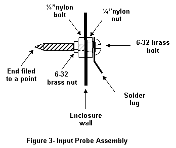
connection is made via a homebrew probe detailed in Figure 3. A nylon machine screw is drilled coaxially
with a clearance hole for a brass 6-32 bolt.
The nylon screw passes through a ¼ inch hole in the case with its head
outside the box and is held in place by a ¼ inch nylon nut on the inside. The 6-32 bolt has its head inside the case
securing a solder lug. It is held in place by a brass nut tightened on the
screw outside the case. The far end of
the brass screw is filed to a conical point for easy circuit probing.
The input probe is connected to the printed
circuit board by the wire soldered to the IN pad. It is also soldered to the
probe solder lug.
The Accuprobe’s RF ground connection is
made through a 3-inch alligator clip lead (wire not supplied with kit) mounted
to a bolt through a clearance hole in the metal case. The hardware stackup is illustrated in Figure
4. A 6-32 bolt protrudes through a hole
in the case next to the input probe. The
screw head is inside the case and holds a solder lug in place. The wire soldered onto this lug goes is one
connected to the GND pad on the pc board.
Outside the case a second solder lug is used to hold the flexible ground
lead. A nut secures the lug to the case. Do not use a longer ground lead since this
can result in inaccurate readings.
The pc board can be mounted in the case
several ways. For very secure mounting,
drill four holes in the tin lining them up with the four corner holes in the pc
board. Be sure, however, to leave room
for the 9-volt battery. Use insulated
standoffs or rubber grommets to hold the board above the metal case so that the
bottom side does not short to the case.
A less formal but more expedient mounting
method is to use double-sided adhesive foam tape commonly used to mount
photographs. It is available at most
full-service chain drug stores, hardware megastores and the ubiquitous Radio
Shacks ™.
The battery can be mounted using the same
adhesive foam tape. It should last for
months so long as the Accuprobe is turned off when not in use so it can be
mounted more or less permanently in this way.
The more adventurous homebrewer can use adhesive-backed Velcro™ strips
to allow easy battery swap out.
DMM output leads pass through a ¼ inch hole
in the tin that has a grommet mounted in it to protect them from abrasion from
the metal. The far ends of the leads are
connected to banana plugs to plug into a DMM.
This wire is not supplied with the kit so be sure to use leads with
different colors so that you can put the black (-) banana plug on the GND lead
and the red (-) plug on the OUT lead.
Checkout
Before connecting a battery for the first
time, ensure that jumpers JU1 and JU2 are in their left-hand position (i.e. the
copyright message is at the bottom of the board) and the power jumper JU3 is
plugged onto only one pin of the terminal block. Connect the output leads to a
DMM, observing correct polarity. The red
plug is positive and the back one is negative.
Set the DMM to read DC voltage on a range
of 10 volts or so. Now set power jumper
JU3 to connect to both leads on the power terminal block. The DMM should read about 10 mV or less. If it reads much higher than this check
connections and ensure that IC U1 is oriented correctly and that all its pins
are making contact with the socket.
To check operation, you will need a
low-level RF source. The best way to
check operation is with a calibrated RF signal generator. Simply load the output of the generator with
its rated load resistance and connect the probe across the resistor. DC readings on the DMM should be the RMS
value of the signal generator output.
Lacking a calibrated signal generator you
can use an oscillator in a receiver.
Clip the input ground lead to a ground point in the receiver close to
the oscillator components and touch the input probe to the output of the
oscillator. You should get a reading in
the 10’s of millivolts to several volts depending on the oscillator output
level. If you have a circuit where the
RF levels are specified you can verify that the readings agree. Otherwise all you will get is a relative
indication.
The Accuprobe’s HIGH range can be checked
using an HF QRP transmitter. Be sure to
set jumpers to the HIGH position with both of them on the right hand set of
terminals. Set the transmitter to output
a known level in the QRP range and assure that it is terminated in a 50 ohm
load. Now clip the Accuprobe ground lead
to a convenient ground point and touch the input probe to the center conductor
of the transmitter output connector. The
DC reading on the DMM will be 1/10th the RMS value of the
transmitter output voltage. At 1 watt
this will be 70.7 mV, ranging up to 158 mV for a 5 watt transmitter.
Be sure to plug power jumper JU3 onto only
one lead of its terminal block when you are done using the Accuprobe to turn
off the power.
Theory of Operation
The Accuprobe is an RF detector with
compensation circuitry that extends accurate readings well below common RF
detector probes. Reference to the
attached schematic diagram shows that it begins with a common AC-coupled
half-wave detector formed by input capacitor C1, Schottky diode D1, resistor R1
and filter capacitor C2. At RF input
levels of several volts or more, the DC across C2 is approximately the peak
value of the input signals. However the
inherent diode non-linearity causes the DC voltage to be less than the peak
voltage at low levels and quite small (only millivolts) when the input RF is
below 100 mV.
For low input levels (the LOW range)
jumpers JU1 and JU2 are connected to the left-hand sets of terminals. Resistor R2 serves as a load for the
half-wave detector. DC from the detector
is fed to operational amplifier U1a through R3.
R3 may appear unnecessary since its resistance is so low that it has
negligible effect, however it prevents damage to U1 from input voltages higher
than the specified range.
Diode D2 provides feedback to the U1a’s
inverting input to compensate for low-signal detector non-linearity. The amount of feedback applied is adjusted by
resistor R4. This compensation scheme is
the brainchild of John Grebenkemper, KI6WX who used it in SWR bridges. W7EL later applied the same technique in QRP
SWR bridges. Their material has appeared
in the ARRL Handbook and QST.
U1a’s output is the corrected peak value of
the input RF voltage. It is fed through
a voltage divider formed by R6 and R7 which convert it to the input’s RMS
value. Again U1b is a unity gain buffer
that feeds a DMM.
For higher voltage levels (the HIGH range)
jumpers JU1 and JU2 are set to connected the right-hand sets of terminals. Resistors R5 and R7 form a voltage divider to
convert the peak DC voltage to the corresponding
Operating power is supplied by a 9-volt
battery. No on-off switch is provided. Instead Jumper JU3 is used to connect two
terminals when plugged onto both leads of the terminal block. Capacitor C3 serves as a power supply bypass
for U1 to prevent instability.
Usage
The Accuprobe is useful for measuring RF
signals with predictable results from 100 kHz to at least 30 MHz at levels
ranging from 10’s of millivolts up to 35 V rms.
It provides minimal circuit loading so that it can be used for signal
tracing in oscillator and mixer circuits as well as multistage QRP
transmitters. Several suggested
applications are:
·
Amplifier input
and output voltages to determine gain
·
Filter input and
output voltages to determine loss
·
Measurement of
resonant circuit or filter circuits across a frequency band to check bandwidth
or Q
·
RF power levels
across a dummy load from microwatts to beyond QRP. Note that a very accurate 50 ohm dummy load
is needed to retain accuracy.
·
Attenuator
calibration by accurate loss measurements.
·
Signal generator
output calibration
·
The Accuprobe
circuit board can also be incorporated into other projects wherever accurate
repeatable RF voltage measurements are needed.
Enhancement Ideas
The Accuprobe can be added to and tailored to
improve its utility and accuracy. A short list of enhancements is:
·
Measure its
output values with a laboratory grade calibrated signal generator and develop a
calibration chart specific to each unit.
Accuracies of 1 or 2 percent are using this method.
·
Panel mount
switches can be used for range switching and power on/off. Use of terminal blocks allows easy
connectorization of the off-board leads.
·
Accuprobe low
frequency response can be extended below 100 kHz by increasing the capacitance
of C1 and C2.
·
A BNC or other
coaxial input connector can be used instead of the probe provided. A Tee connector on this input connector would
ensure that a good 50 ohm termination could be made for accurate power readings
in a coaxial cable hookup.
·
Diodes D1 and D2
can be matched for improved accuracy below inputs of 100 mV RMS.
·
A small
adjustable bias circuit could be added to null out the inherent operational
amplifier offset voltage for improved accuracy with small input signals.
·
The Accuprobe
can be interfaced with a precision analog to digital converter, a
microcontroller and numeric display to build a dedicated RF voltmeter or RF
wattmeter. Calibration values could be
measured and stored in the microcontroller memory to provide improved
measurement accuracy.
·
Analog meter
fans can also add an external analog DC meter with appropriate ranges to make
an analog RF voltmeter or RF wattmeter.
Credits
The Accuprobe project was
conceived and promoted by Doug, KI6DS who also provided necessary prodding and
encouragement. AmQRP provided funding
for prototype development. Printed
circuit layout was masterfully carried out by Lenny, W2BVH. Circuit design and checkout was performed by
Joe, N2CX. Technical questions on the
Accuprobe can be directed to him at n2cx@amqrp.org.
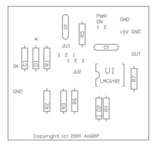
Figure 1 – Accuprobe Component Layout
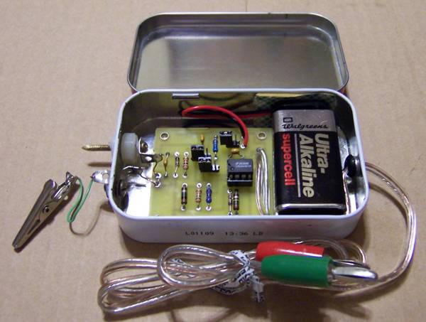
Figure 2 – Accuprobe Prototype installed in Altoids ™ mint tin

Figure 4 – Accuprobe Schematic Diagram